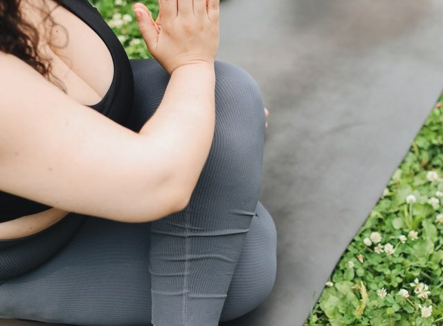
Plus size women’s workout clothes can be tough to find. But don’t worry, we’ve got you covered with the best shopping tips for plus-size women’s workout clothes. With the right strategy, these buying tips will help you find the perfect outfit that you’ll love and wear again and again. Whether you’re looking for something short or long sleeve, a tee or a dress, our buying guide will show you how to buy workout clothes that fit just right and make your exercise routine feel as easy as possible.
Understand the best types of workout clothes
There are many different types of workout clothes. Plus size women should understand the best types of workout clothes for their needs so that they can find the perfect outfit to wear during workouts. The type of garment you Best Buy hacks is likely going to depend on how intense or long your workout routine is, and what you want to wear it for. If you’re only looking for a quick workout, then you’ll probably be fine with a tank top and shorts. But if you’re looking for something more long-lasting, then a tee and leggings will do the trick.
Know what to look for in your workout clothes
Short versus long sleeve
Tops versus bottoms
T-shirts versus dress
It can be difficult to find the perfect workout outfit, but with the right knowledge, it is possible. When shopping for your workout clothes, focus on three main areas: what to look for in your clothing, what to look for in sizing and how to know if you’ll wear your outfit enough to make it worth it.
First things first, what should you look for in your clothing? One of the most important features is whether or not the clothes are moisture-wicking. These pieces will help keep you cool when you’re working out. Another important consideration is whether or not the material is breathable. You want something that’s comfortable and doesn’t overheat or cause chafing while exercising. Fabrication also plays an important role in how well a piece will work during exercise. Make sure that your clothing has stretchy fabrics so that they won’t feel restrictive as you move around.
Find the perfect size for you and your exercise routine
The first thing you’ll want to do is find the perfect size for yourself and your exercise routine. Do you like your workout clothes to be form-fitting? Tight? Loose? If your answer is yes to any of these, then you need Best buying tips a smaller size. If your answer is no, then don’t worry about sizing and go for a regular fit.
When it comes to plus-size women’s workout clothes, most people often try on multiple sizes before deciding on the correct one. This isn’t necessary! Just make sure you know what type of clothing will give you the best results and go from there.
Tips on buying plus size workout clothes
When shopping for plus-size women’s workout clothes, there are a few important things to keep in mind. First of all, it is best to shop at physical stores rather than online. This makes it easier for you to try on different items and find the perfect fit. Second, make sure that whatever you get fits your needs well. And last but not least, make sure that the price is right.
The best brands for plus size women’s workout clothes
If you’re looking for the best brands for plus-size women’s workout clothes, you need to know what features to look for in a brand. The first thing is sizing. Plus size women’s workout clothes are available in different sizes and shapes. They range from extra-small to large. These are the brands that offer plus-size options:
Gap: Gap has clothing from XS to 3X, so there’s something for everybody and the budget.
American Eagle Outfitters: AE offers stretchy cotton, high-quality materials, and a wide selection of styles, like crop tops and tanks.
Nike: Nike offers high-quality, fashion-forward pieces that are designed for all types of workouts.
H&M: H&M offers a wide selection of plus-size options, including activewear as well as everyday casual attire.
Aerin Athletica: Aerin is a great place to shop if you’re looking for professional sports apparel with an activewear twist at an affordable price point.
Of course, not every brand will have everything on this list, but these are some of the good brands out there when it comes to plus-size women’s workout clothes.
Conclusion
If you want to get the most out of your workout routine, you need the right clothing. When buying plus-size workout clothes, it’s important to know the best types and what to look for. With this guide, you’ll be confident in your pick of work-out clothes that are going to help you do your best.